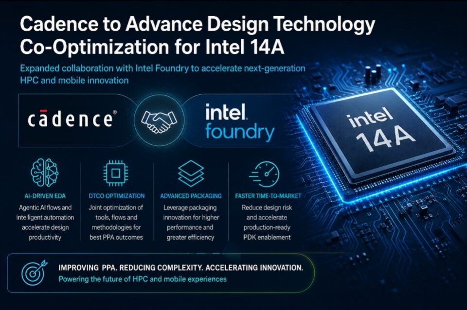
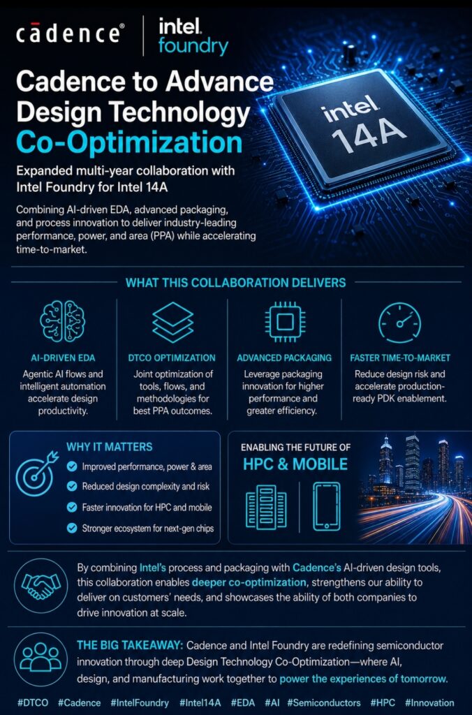
Cadence to Advance Design Technology Co-Optimization through an expanded multi-year collaboration with Intel Foundry focused on Intel 14A process technology. The partnership combines AI-driven design automation, advanced packaging, and manufacturing expertise to improve performance, power, and area outcomes while helping customers accelerate next-generation HPC and mobile innovation.
The Next Semiconductor Race Is No Longer About Nodes Alone
Cadence to Advance Design Technology Co-Optimization may sound like a technical announcement aimed primarily at chip engineers. Yet the deeper significance extends far beyond semiconductor design.
The semiconductor industry is entering a period where traditional scaling advantages are becoming harder to achieve. Customers want faster AI systems, more efficient mobile devices, lower power consumption, and shorter product development cycles. At the same time, engineering complexity continues to rise.
Against this backdrop, Cadence and Intel Foundry have announced an expanded multi-year collaboration targeting Intel’s next-generation process technologies beginning with Intel 14A. The partnership combines Cadence’s agentic AI-driven EDA and Design IP portfolio with Intel Foundry’s process and packaging innovations.
The objective is clear: improve performance, power, and area while reducing design complexity and accelerating time-to-market.
However, the strategic story is much larger than tool optimization.
Why Cadence to Advance Design Technology Co-Optimization Matters Now
For decades, semiconductor innovation followed a relatively straightforward model.
Foundries advanced manufacturing processes. Design teams created increasingly sophisticated chips. EDA vendors supplied the tools needed to translate architectures into manufacturable products.
The boundaries between these participants were relatively clear.
Today, those boundaries are disappearing.
Advanced nodes require tighter coordination between design methodologies, manufacturing processes, packaging technologies, verification workflows, and AI-driven optimization. Small inefficiencies can translate into millions of dollars in development costs and significant market delays.
This becomes critical when AI infrastructure demand is accelerating globally.
Enterprises deploying large-scale AI systems need predictable performance improvements. Mobile manufacturers require greater energy efficiency. High-performance computing providers must maximize compute density while controlling power consumption.
The old model of sequential optimization is increasingly inadequate.
The new model is co-optimization.
A Strategic Expansion Rather Than a Conventional Partnership
The announcement signals a deeper relationship between Cadence and Intel Foundry.
“Advancing our relationship with Intel into a much deeper partnership is a major milestone for both companies,” — Anirudh Devgan, President and Chief Executive Officer, Cadence.
Rather than simply certifying tools for process compatibility, the companies are working together earlier in the technology lifecycle.
This approach allows manufacturing realities, packaging innovations, and design requirements to influence one another from the outset.
Strategically, this indicates a shift in capability ownership.
Success is no longer determined by a single organization delivering a breakthrough technology. It increasingly depends on how effectively ecosystem participants coordinate innovation across multiple domains.
For Intel Foundry, the collaboration strengthens ecosystem confidence around its technology roadmap.
For Cadence, deeper process integration creates opportunities to embed AI-driven intelligence directly into next-generation design flows.
Competition Is Moving Toward Ecosystem Excellence
The semiconductor industry has already entered an ecosystem competition phase.
Synopsys continues expanding AI-assisted design capabilities. Siemens EDA is investing heavily in verification, digital twins, and advanced packaging technologies.
Meanwhile, Intel Foundry competes against established ecosystem leaders including TSMC and Samsung Foundry.
The challenge is no longer simply delivering a superior process node.
The challenge is enabling customers to successfully design products for that process node.
This distinction is increasingly important.
Customers evaluate manufacturing ecosystems based on available IP, design enablement, tool support, validation readiness, and implementation certainty.
The organizations that simplify customer innovation will gain competitive advantage.
How the Technology Stack Comes Together
At its core, Design Technology Co-Optimization creates continuous feedback loops between design and manufacturing.
Intel Foundry contributes process technology, manufacturing expertise, and packaging innovations.
Cadence contributes EDA platforms, Design IP, verification capabilities, and implementation workflows.
The most transformative element may be the integration of agentic AI.
AI-driven design systems can evaluate design trade-offs, identify bottlenecks, automate optimization decisions, and accelerate engineering workflows.
The result is a more integrated development environment where process constraints and design objectives evolve together.
Operationally, this translates into faster design convergence, reduced engineering iterations, and lower implementation risk.
The value is not simply automation.
The value is orchestration.
The Customer Experience Begins Long Before Product Launch
From a CX standpoint, semiconductor announcements are often underestimated.
Customers rarely interact directly with design automation software or manufacturing process technologies.
Yet they experience the outcomes every day.
Faster application responsiveness, improved battery life, reduced latency, better AI performance, and enhanced reliability all originate from semiconductor-level decisions.
When DTCO improves performance, power, and area metrics, those improvements cascade upward through devices, software platforms, and digital services.
The customer experiences the result without ever seeing the underlying engineering.
This is why semiconductor optimization increasingly represents a customer experience strategy rather than merely a technical initiative.
At a structural level, the collaboration demonstrates how customer outcomes are becoming linked to ecosystem coordination. The organizations that reduce engineering friction are often the same organizations that ultimately improve end-user experiences.
The Industry Is Approaching a New Maturity Curve
The collaboration also highlights the evolution of semiconductor operating models.
Historically, organizations optimized individual stages of development.
Today, leading companies are optimizing ecosystems.
The next stage will likely involve AI systems continuously coordinating decisions across design, manufacturing, packaging, verification, and deployment environments.
Such a model would move beyond collaborative DTCO toward adaptive optimization at scale.
Organizations capable of reaching that level first could achieve significant competitive advantages.
The deeper implication is that semiconductor innovation is becoming increasingly dependent on the quality of ecosystem intelligence rather than isolated technical breakthroughs.
Decision Makers Should Focus on Ecosystem Leverage
The announcement provides an important lesson for technology leaders.
Building every capability internally is becoming increasingly difficult.
The complexity of modern semiconductor development requires access to expertise across multiple domains.
For many organizations, partnership-based ecosystem participation offers a more practical route to innovation than attempting to build all capabilities independently.
This is particularly true for companies pursuing AI, HPC, and next-generation mobile opportunities.
The ability to leverage ecosystem strengths may ultimately become more important than ownership of any single capability.
Organizations evaluating future semiconductor strategies should increasingly assess ecosystem readiness, design enablement, AI integration, and manufacturing alignment alongside traditional performance metrics.
Looking Ahead
“By combining Intel’s process and packaging with Cadence’s AI-driven design tools, we are enabling deeper co-optimization, strengthening our ability to deliver on customers’ needs, and showcasing the ability of both companies to drive innovation at scale.” — Naga Chandrasekaran, Executive Vice President and General Manager, Intel Foundry.
That statement captures the broader significance of the collaboration.
The semiconductor industry is transitioning from isolated innovation toward coordinated innovation.
Future success will increasingly depend on how effectively organizations align manufacturing, design, AI, packaging, and ecosystem capabilities around shared customer outcomes.
Cadence to Advance Design Technology Co-Optimization therefore represents more than a technology announcement.
It reflects a broader industry shift toward ecosystem-centric innovation, where customer value is created through collaboration, orchestration, and continuous optimization across the entire semiconductor value chain.
Key Takeaways
- DTCO is evolving into a strategic competitive differentiator.
- AI-driven design automation is moving closer to manufacturing enablement.
- Ecosystem strength is becoming as important as process leadership.
- Customer experience improvements increasingly originate at the silicon layer.
- The Cadence–Intel Foundry collaboration reflects the future direction of semiconductor innovation. :::